Axio Electronics excels in cutting-edge PCB design and hardware engineering, offering fully customized solutions tailored to complex applications. Our expertise includes mixed-signal boards, high-speed digital design, analog circuit design, PCB simulation, and seamless electronic component integration.
From concept to production, we ensure precision, performance, and innovation at every stage.

Electronics development is at the core of product innovation, enabling businesses to launch cutting-edge digital devices that meet evolving market demands. At Axio Electronics, we drive technological advancements by enhancing the functionality and capabilities of digital products across industries.
Our development process is built on a systematic, thorough approach—guiding projects from concept to production with precision. We collaborate closely with clients, leveraging state-of-the-art tools and facilities to design, develop, and manufacture high-quality technology. Our in-house PCB printing technology, including Voltera V-One, allows us to rapidly validate hardware prototypes in just a week, significantly accelerating the development cycle.
Our holistic methodology ensures a smooth, efficient product development cycle, covering key stages:
- Technology Research & Component Selection
- Circuit Design & Simulation
- Schematics Design
- PCB Layout & Simulation
- Rapid PCB Prototyping & Hardware Validation
- PCBA Prototyping & Initial Testing
- Engineering Validation Testing (EVT)
- Design Validation with Contract Manufacturer (DVT)
- Production Validation Testing (PVT) & Mass Production Launch
OUR CASE STUDY
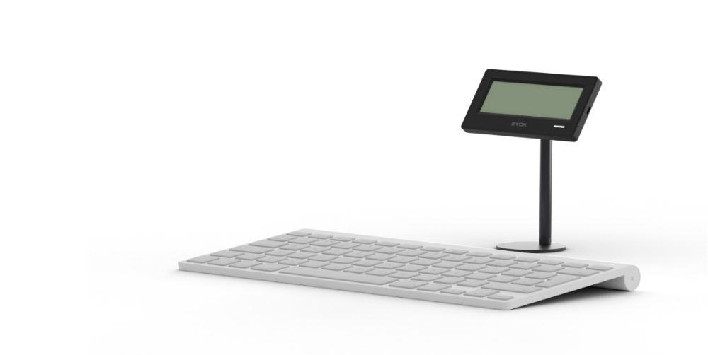
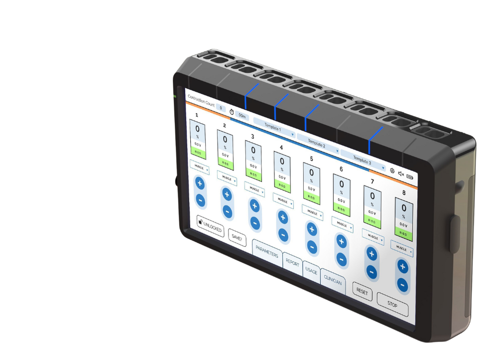
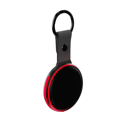
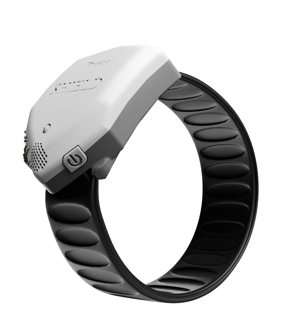
PCB Design & Hardware Guide & Timeline

Finalize Requirements
1 weekBlock Diagram & Schematic Draft
1 weekComponent Selection & Footprints
1 weekSchematic Review & Sign-off
3 weeksPCB Layout & Constraints
3 weeksFabrication + Assembly Order
Depends on ManufacturingBring-up & Hardware Validation
2 weeksExpert Engineering Team & Comprehensive Development Process
Our engineering team defines goals, selects technologies, and creates a roadmap. We collaborate with firmware, CAD, and procurement specialists for seamless integration.
With expertise from over 50+ successful projects, we guarantee a technically and financially viable product development journey.
CIRCUT DESIGN & SIMULATION
Prepare a block diagram based on specifications. Conduct power analysis and generate a major Bill of Materials (BOM).
Innovate electronics hardware and simulate circuit designs. Generate detailed reports for analysis and validation.
Tech Stack & Tools Used:
Block Diagram & Documentation: Notion, Google Drive
Power Analysis & Simulation: LTspice, PSpice, MATLAB, Simulink
BOM Management: Altium Designer, Octopart, Ultra Librarian

CUSTOM PCB DESIGN
TESTING & VALIDATION
Conducting EVT, DVT, and PVT testing with thorough documentation to ensure reliability and production readiness.
Tools Used:
Testing Equipment: Oscilloscopes, Multimeters, Logic Analyzers, Thermal Imaging Cameras
Simulation & Validation: ANSYS, COMSOL Multiphysics,
How we communicate?
Bi-weekly technical calls, Weekly PDF reports, Robust version control, project management access
Deliverables
(Timeline - 4-6 Weeks)*
- Functional Prototype – Fully assembled and working hardware for testing and evaluation.
- Validated PCB Design – Production-ready PCB layout with optimized schematics.
- Manufacturing Package – Complete set of Gerber files, BOM, assembly drawings, and test procedures.
- Tested & Certified Hardware – Hardware validated through EVT, DVT, and PVT stages, ready for production.
- Scalable Production Plan – Supplier-ready documentation for seamless mass manufacturing.
DOWNLOAD SAMPLE
PCB DESIGN & HARDWARE
DOCUMENTS
We prepare for next steps
Prepare development plan from idea to manufacturing
Get a financial proposal for development
Frequently asked questions
What can a PCB design scope include?
A PCB scope can include requirements review, component selection, schematics, board layout, fabrication outputs, assembly information and bring-up support. Specify editable files, BOM, test points and acceptance evidence in the agreed deliverables.
Can you review or redesign an existing PCB?
Share the board revision, schematics, layout files, BOM, known failures and measurements. A review can then focus on documented problems such as power behavior, interfaces, component availability or assembly constraints.
What is needed before PCB fabrication?
Review the approved schematic and layout revision, stack-up and fabrication constraints, BOM availability, assembly outputs and intended test access. Confirm the manufacturing package with the selected supplier before ordering.
What should I share before requesting a proposal?
Share the problem to solve, intended users, product stage, required functions, operating environment and target quantity. Existing drawings, board files or test results help define the next engineering step.
Who owns the design files and source code?
Ownership, licensing, third-party components and handover files are defined in the project agreement. Agree these terms before development starts, including access to editable design files and source code.
How are development cost and schedule estimated?
The estimate depends on scope, technical uncertainty, prototype iterations, component availability and validation needs. An enquiry starts a scope discussion; it is not a fixed quote or a promised delivery date.
LET'S TALK ABOUT YOUR PROJECT.
PLEASE FILL OUT THE FORM AND WE'LL GET BACK TO YOU SHORTLY.
 Axio Electronics
